

Scientists have explained the mechanism of formation of materials for a new generation of optoelectronic devices
The physicists from the Institute for Problems in Mechanical Engineering of the Russian Academy of Science, St. Petersburg State University, the Higher School of Economics and the Academic University named after J.I. Alferov studied the mechanism of formation of three-dimensional structures on a promising semiconductor indium-galium-nitride alloy. The research will help in developing a new generation of non-planar optoelectronic devices in the field of electronics and communications.
The results of the study were published in ACS Applied Nano Materials.
InGaN (indium-galium-nitride) – alloy is a semiconductor material consisting of a mixture of gallium and indium nitrides. White and blue LEDs are made on the basis of this alloy. This material is promising for creating gas sensors, solar cells, cells for hydrogen synthesis, red, green and white LEDs, and much more. However, the material is not widely used now, since InGaN layers are difficult to synthesize due to the phenomenon of «solubility gap». This phenomenon is characterized by the fact that InGaN is unstable and decays into separate phases InN and GaN. And it is difficult to integrate it with a silicon platform due to the difference in permanent crystal lattices between these materials. The synthesis of a material directly on the silicon surface in a complex form, in the form of filamentous nanocrystals, nanoflowers and other forms, can solve these problems. This variant of alloy synthesis also expands significantly the potential of using this material to create devices.
Joint research by the physicists from St. Petersburg University, the Academic University named after Zh.I. Alferov, the Institute for Problems in Mechanical Engineering of the Russian Academy of Sciences and the Higher School of Economics helped to understand the mechanism of formation of these complex three-dimensional nanostructures, otherwise their synthesis would be impossible.
“For the first time, we were able to explain the complex mechanism of formation of three-dimensional (non-planar) structures based on InGaN material by applying scientific and systematic approaches to describing the growth processes of this structure. Based on such compounds, the prototypes of LEDs, gas sensors, water decomposition cells and more are already being created in the Laboratory of the St. Petersburg State University. Understanding the mechanisms of formation of these complex three-dimensional nanostructures may contribute to the development of a new generation of non-planar optoelectronic devices”, Rodion Reznik, Head of the Laboratory of New Semiconductor Materials for Quantum Informatics and Telecommunications at St. Petersburg State University, told.
According to him, this compound is obtained by molecular beam epitaxy (MBE), a method which allows you to grow the heterostructures with desired properties in ultrahigh vacuum conditions. The method allows to create efficient new generation of devices.
In case of synthesis of nitride compounds using a research facility, the synthesis process by molecular beam epitaxy is quite long, however, the output is a large plate which can be cut into hundreds of small pieces, each of which is a base for a device.
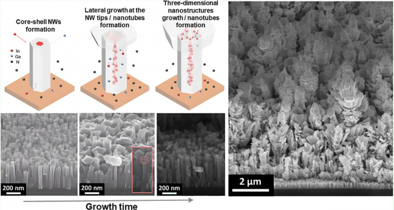
Sergey Kukushkin, the Head of the Laboratory of Structural and Phase Transformations in Condensed Media at IPMash RAS, was engaged in building a theoretical model of a complex phenomenon — the formation of InGaN nanoflowers. The process of growth of InGaN nanocrystals on silicon by the MBE method is complex and multistage. It involves the spontaneous «construction» of nanostructures consisting of a hollow tubular nanocrystal covered with a crystalline «cap». This process takes place without outside interference.
The reason for the growth of branched nanostructures, similar to a bouquet of flowers, is that the indium atoms included in the InGaN solid solution are much larger than gallium atoms. In addition, indium nitride decomposes well into indium and nitrogen atoms at the growth temperature. As a result of the decomposition of indium nitride, droplets of metallic indium are formed, which easily evaporate from the substrate. Since the lattice parameters of the substrate are greater than the lattice parameters of the solid solution, tensile elastic stresses arise in the solid solution layer. Indium tends to compensate for this stress and moves in the direction of the maximum stretching of the crystal.
“In the process of growing, the indium atoms evaporating from the indium metal move inside the cavity. And with an increase in the height of the nanocrystal, the influence of the substrate decreases, and a «cap» is formed on the surface of the nanocrystal, consisting of a solid solution of indium and gallium with a predominance of indium. As it grows, the diameter of the «cap» increases and begins to exceed the diameter of the nanocrystal. As a result, the «cap» begins to «feed» from the gas phase. At the same time, only certain facets of the crystal have the highest growth rate," explained Sergey Kukushkin.
The scientists of the Laboratory of Structural and Phase Transformations in condensed media of IPMash RAS have been researching silicon-based nanomaterials for more than 20 years.
A fundamentally new type of monocrystalline silicon carbide cultivation on silicon has been created, which can lead to the creation of a new type of high-capacity electrodes.