

IPMash RAS are the first in RF to create technology of production of material for microelectronics of the future
The basis of modern electronic devices, computers, communication devices, sensors, transmitting and playback equipment are microcircuits made on the basis of semiconductor materials. Silicon is one of the main materials on the basis of which most of the various devices are currently manufactured and, in particular, such as: LEDs, semiconductor lasers, solar panels, mobile phones, satellite TV, radars, refrigerators, washing machines, microwave ovens and video equipment. An important advantage of silicon is the ease of processing. The production of silicon wafers for chips and microcircuits, polishing, cleaning and cutting them are well mastered all over the world and therefore devices made on the basis of silicon wafers are inexpensive.
The main disadvantages are that silicon-based semiconductor devices work stably only in a narrow temperature range, and do not withstand radiation exposure well.
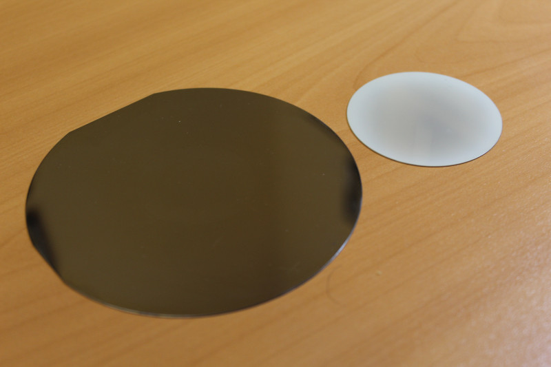
Silicon carbide (a compound of silicon with carbon) can become one of the most promising materials capable of replacing silicon, without abandoning its manufacturing technologies brought to perfection.
“As a result of our research, a fundamentally new method of growing monocrystalline silicon carbide on silicon was discovered. The method is based on the coordinated substitution of a part of the atoms in silicon for carbon atoms without destroying the silicon base. For the first time in world practice, a self-consistent coordinated substitution of atoms of one grade for other atoms directly inside the initial crystal without destroying its crystal structure has been implemented. The quality of the structure of the layers obtained by this method exceeds significantly the quality of films grown on silicon substrates by leading global companies. The method is cheap and technologically advanced", says Sergey Arsenyevich Kukushkin, Head of theIPMash RAS Laboratory of Structural and Phase Transformations in condensed matter.
The main problem faced by the scientists was that with the standard growth of silicon carbide film on silicon, the crystal structure of silicon carbide does not coincide with the crystal structure of silicon. As a result, the silicon carbide film cracks. The atoms did not fall into place, mechanical stresses arose, and the film cracked. In this form, it becomes unsuitable for the manufacture of devices.
Then the scientists realized that it was necessary to «remove» some of the atoms in the substrate, that is, to create empty spaces in the crystal lattice of the substrate due to the formation of so-called «vacancies» in it. The main difficulty was to create vacancies at that very moment of the film's origin, precisely when the vapor sprayed from the external environment begins to turn into a silicon carbide film.
The scientists considered it most correct to replace some of the atoms in silicon with carbon, that is, to immediately turn silicon into silicon carbide without destroying it. According to theoretical research, if a carbon atom is placed in the voids on the silicon surface, and the silicon atom next to it is removed, it turns out that the dimensions of the silicon crystal lattice containing such defects will almost coincide with the dimensions of the silicon lattice without defects. That is, there will be no mechanical stress.
«The theoretical calculations have been fully confirmed in practice. We had to find such a chemical substance, as a result of interaction with which a carbon atom would be embedded in the silicon lattice, but so that the chemical reaction would not proceed immediately before the formation of silicon carbide, but an intermediate structure would be formed. And we found such a substance. It turned out to be ordinary carbon monoxide. Realizing this, we began to grow single-crystal silicon carbide films on silicon, which today surpass (in structure and composition) silicon carbide films on silicon grown by the world's main leaders in the field of electronic materials! And most importantly, cost of our films is more than ten times lower than the cost of these films,» explained Sergey Arsenyevich Kukushkin.
This study opens up many prospects for the use of silicon carbide.
On such substrates it is possible: to grow transistors with high mobility of charge carriers, to grow heterostructures of gallium nitride for blue lasers, to use them as a basis for quantum computers, to create domestic microchips for LEDs, to create ultra-efficient sensors, to create terahertz radiation receivers for lung diseases, and devices for post-stroke and post-infarction therapy, to create a device “burning” excess sugar in people with diabetes.
In addition, devices that use silicon carbide can operate at almost three hundred degrees Celsius without loss of semiconductor properties, while silicon melts already at temperatures exceeding 60 degrees Celsius. Finally, silicon carbide microchips can operate under conditions of high radiation exposure, i.e. at nuclear power plants and in space.
The technology can form the basis of high-tech production of single-crystal silicon carbide layers on silicon substrates.
This would make it possible for Russia not only to substitute the import of foreign semiconductor structures, which have no analogues in Russia, but also to act as a global technological leader in the field of development of new-generation semiconductors.